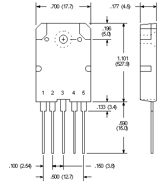
| Straight Leads | Formed Leads |
 |
 |
| Note: You may receive either case style. | |
| Peak Input Voltage, VIN | 850V | |
| Input Current, IIN Continuous Pulse |
6A 12A | |
| Maximum Output Current (VO = 115V), IO | 1.3A | |
| Power Dissipation (TC = +100°C), PD | 27W | |
| Power Transistor Junction Temperature, TJ | +150°C | |
| Operating Temperature Range (TC), Topr | -20° to +125°C | |
| Storage Temperature Range, Tstg | -30° to +125°C |
Electrical Characteristics: (TA = +25°C unless otherwise specified)
| Parameter | Symbol | Test Conditions | Min | Typ | Max | Unit |
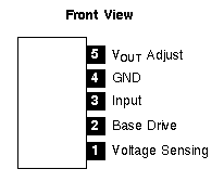
| Output Voltage | VO | VIN = 220V, IO = 900mA, Note 2 | 108.5 | 110.0 | 111.5 | V |
| Sensing Voltage (Fixed Voltage) | VO | IIn = 7mA | 41.3 | 41.8 | 42.3 | V |
| Line Regulation | RegLINE | VIN = 180V to 280V, IO = 900mA | Initial Value ±1 | V | ||
| Load Regulation | RegLOAD | VIN = 220V, IO = 550mA to 900mA | Initial Value ±2 | V | ||
| Output Voltage Temperature Coefficient | TC = -20° to +100°C, IIn = 7mA | - | ±2 | - | mV/°C | |
| Saturation Voltage | VCE(sat) | IC = 3A, IB = 600mA | - | - | 0.4 | V |
| VBE(sat) | IC = 3A, IB = 600mA | - | - | 1.5 | V | |
| DC Current Gain | hFE | IC = 1A, VCE = 4V | 15 | - | 38 | |
| Collector Cutoff Current | ICEX | VCE = 850V, VBE = 1.5V | - | - | 1 | mA |
| Power Transistor Thermal Resistance | RthJC | Between Junction and Stem Upper Surface | - | 1.8 | - | °C/W |
| Switching Time | ts | IC = 3A, IB1 = 500mA, IB2 = -500mA, RL = 67 Ohms |
- | - | 11.0 | µs |
| tf | - | - | 0.5 | µs | ||
| Note 1. | Recommended Case Temperature: Topr = +100°C. |
| Note 2. | Output voltage is determined by the ratio between the sensing winding "D" and the secondary winding "S". |
| Straight Leads | Formed Leads |
|
|
| Note: You may receive either case style. | |
