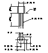
Absolute Maximum Ratings: (TA = +25°C unless otherwise specified)
| Power Dissipation, PD | 300mW | |
| Derate Above 25°C | 3.0mW/°C | |
| RMS Emitter Current, IE(RMS) | 50mA | |
| Peak Pulse Emitter Current (Note 1) Current, iE | 1.5A | |
| Emitter Reverse Voltage, VB2E | 30V | |
| Interbase Voltage, VB2B1 | 35V | |
| Operating Junction Temperature Range, TJ | -65° to +125°C | |
| Storage Temperature Range, Tstg | -65° to +150°C |
| Note 1. | Duty Cycle </= 1%, PRR = 10PPS. |
| Note 2. | Based upon power dissipation at TA = +25°C. |
| Parameter | Symbol | Test Conditions | Min | Typ | Max | Unit |
| Intrinsic Standoff Ratio | VB2B1 = 10V, Note 3 | 0.70 | - | 0.85 | - | |
| Interbase Resistance | rBB | 4.0 | 6.0 | 9.1 | k Ohms | |
| Interbase Resistance Temperature Coefficient | 0.1 | - | 0.9 | %/°C | ||
| Emitter Saturation Voltage | VEB1(sat) | VB2B1 = 10V, IE = 50mA, Note 4 | - | 2.5 | - | V |
| Modulated Interbase Current | IB2(mod) | VB2B1 = 10V, IE = 50mA | - | 15 | - | mA |
| Emitter Reverse Current | IEB20 | VB2E = 30V, IB1 = 0 | - | 0.005 | 1.0 | µA |
| Peak Point Emitter Current | IP | VB2B1 = 25V | - | 1 | 5 | µA |
| Valley Point Current | IV | VB2B1 = 20V, RB2 = 100 Ohms, Note 4 | 4 | 7 | - | mA |
| Base-One Peak Pulse Voltage | VOB1 | 5 | 8 | - | V |
| Note 3. | Intrinsic standoff ratio is essentially constant with temperature and interbase voltage and is defined by the equation: VP - VBB + VD where: VP = Peak Point Emitter Voltage; VBB = Interbase Voltage; VD = Junction Diode Drop (~0.5V) |
| Note 4. | Use pulse techniques: Pulse Width ~ 300µS, Duty Cycle </= 2% to avoid internal heating due to interbase modulation which may result in erroneous readings. |
 Home
Back